


Optical Device and Module Fabrication Facilities
Optical Device and Module Fabrication Facilities
Fume Hood
Wafer Cleaning, Electrode Peeling
Mask Aligner
Photolithography (Micron-Order Patterning)
Sputtering Equipment(For Deposition)
Thin Metal Deposition
Surface Profiler
Thickness Measurement for Resist Films & Thin Metal Films
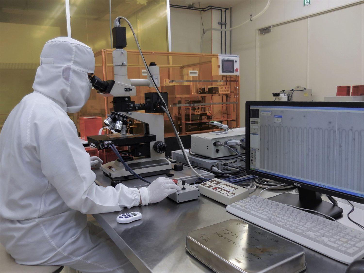
Automatic Line Width Measuring Equipment
Measurement of Electrode Width and Duty Cycle of Periodical Polarization
Electric Field Poling System
Manufacture of Periodically-Poled Structures by Applying High Electric Field
Annealing Oven
Removal of Optical Distortion after Periodic Poling Process
Cleanroom
Class 1000
Laser Spot Welding Machine
Seam Welding Machine
Providing proactive service on various processes and measurements levaraging equipment portfolio as shown above.
Optical Device Measurement and Evaluation Facilities
Life-time Testing System
Long-term Reliability Testing for Non-Linear Frequency Conversion Devices such as QPM
Characterization System for QPM Waveguide
Characterization of Phase-Matched Wavelength, Conversion Efficiency, and Guided Mode Profile for QPM (PPMgLN) Waveguide
Optical Lossmeter
LossPro™ System by NovaWave Technologies,Inc. / Measurement of Optical device Loss (1064,532,355 nm)
Photo-Thermal Common Path Interferometer
PCI-3 System by Stanford Photo-Thermal Solutions / Evaluation of Laser Absorption of Optical Materials and Wafers
Details